[ad#200-link]Deputy Central Intelligence officer Technical Recruitment (DCIO) Test. Exam Question paper, Sample Paper of Deputy Central Intelligence officer Technical Recruitment Below.
Deputy Central Intelligence Officers (Technical) : 10 posts (OBC-3, SC-1, ST-1) in Intelligence Bureau, Ministry of Home Affairs, Age : 35 years. relaxation as per rules, Pay Scale : Rs. 15600 – 39100 grade pay Rs.6600
Qualifications : Essential : Educational : Bachelor’s degree in Electronics Engineering or Electronics and Communication Engineering or Electronics and Tele-communication Engineering or Aeronautics Engineering or Chemical Engineering or Mechanical Engineering or Computer Science / Engineering or B.E./B.Tech. in Information Technology or Master’s degree in Computer Applications or M.Sc in Chemistry or M.Sc in Bio-Technology or M.Sc in Space Engineering and Rocketry or M.Sc in Physics with Wireless or Electronics or Optics or Nuclear Physics as a subject from a recognized University or equivalent.
Duties : To supervise the work relating to operation and maintenance of communication network. Maintenance and operation of equipment relating to cyber security/cyber forensics. Research & Development work, mainly dealing with electronics and telecommunication. To undertake & supervise the operational work assigned. Responsibilities for Supervision, maintenance of communication equipments. To supervise the maintenance and operation of audio, video and CCTV equipments
Note: A Written Objective Type Test with multiple choices answer will be conducted and followed by Interview for selection of Candidates to the posts of Deputy Central Intelligence Officer (Technical). The written test will be conducted on 20th June, 2010 in the Afternoon Session.
Scheme and Syllabus For The Test: Scheme: The test will be of two hours’ duration and the medium of the question paper will be English only. The test will be an objective type with multiple choices of answers and will carry maximum of 100 marks. There will be a penalty for wrong answers. Every wrong answer will carry a deduction of one-third of the marks assigned to that question. If no answer is marked for a question, there will be no penalty for that question
Syllabus: Syllabus of the Test comprises the following :- Scientific temper relating to basic understanding of Science including everyday observation & Experience, Instrumentation, Fundamentals of Basic Electronics, Fundamentals of Computerization and Network, Aptitude Data interpretation, Communication Skills, Basic Questions on Maintenance, Current events regarding Science and Technology, Data & image interpretation, Fundamentals of information security
Application Fee : Fee payable is Rs.50/- in the shape of Central Recruitment Fee Stamp only.
Advertisement Details: http://upsc.gov.in/recruitment/advt/2010/spl50_2010.htm
EXAM PAPER OF 2010 Held on 22/06/2010


what would be the cutoff marks for 7 posts of DCIO/tech exam held on 7-8-2011
Hi All,
Please update all the Answer’s key of all Questions of “seven post of deputy central intelligence officer technical held on dated-07.08.2011”.
And When the 7 post DCIO result is supposed to be out.
Please Revert.
Thanks & Regards
Abhishek
Hi All,
When the 7 post DCIO result is supposed to be out ….. how do i get to know ?
Thanks in Advance,
Ashis
SEVEN POST OF DEPUPTY CENTRAL INTELLIGENCE OFFICER (TECHNICAL) IN INTELLIGENCE BUREAU, EXAM CODUCTED BY UPSC ON DATED -07.08.2011
UPLOADED BY- PRABIRA KUMAR SETHY MTECH IN COMM. ENGG.
ENGGINEERING ASSISTANT [prabirserthy.05@gmail.com]
CENTRAL PRODUCTION CENTRE , DOORDARSHAN, ASIAD VILLGE COMPLEX , NEW DELHI-49
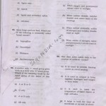
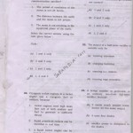
1. A diode for which you can vary the revese bias, and thus vary the capacitance is called
a. Varactor diode
b. Tunnel diode
c. Zener diode
d. Switching diode
Ans- varactor diode
2. A non-volatile type of memory that can be programmed and erased in sectors, rather than one byte at atime is
a. Flash memory
b. EPROM
c. EEPROM
d. MPROM
Ans-EEPROM
3. To get a negative source voltage in a self biased JFET circuit, one must use a
a. Voltage divider
b. Source resistor
c. Bleeder resistor
d. Negative gate supply voltage
ANS- SOURCE RESISTOR
4. An amplifier with resistive negative feed back has two left half planes poles in its open-loop transfer function. The amplifier
a. Will always be unstable at high frequency
b. Will be stable for all frequency
c. May be unstable, depending upon the feed back factor
d. Will oscillate at low frequency
Ans- will be stable for all frequency
5. In the h-parameter model of representing a transistor the input and output sections are modelled as
a. Voltage source
b. Current source
c. Input section as voltage source, and output section as current source
d. Input section as current source and output section as voltage source
Ans-input section as voltage and out put section as current source
6. A differential amplifier is invariably used in the input stage of all op-amp. This is done basically to provide the op-amp a very high
a. CMRR
b. Band width
c. Slew rate
d. Open-loop gain
Ans-open-loop gain
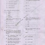
7. In the amplifier, transistor inter-junction capacitance causes
a. Phase shift
b. Harmonic distortion
c. Noise
d. Parasitic oscillation
Ans-parasitic oscillation
8. The loss in signal power as light travels through the optical fiber is called
a. Attenuation
b. Propagation
c. Scattering
d. Interruption
Ans-attenuation
9. The upper cut-off frequency of a transistor amplifier depends upon
a. Coupling and emitter bypass capacitance
b. Junction and wiring capacitance
c. Coupling and wiring capacitance
d. Junction and emitter bypass capacitance
Ans-coupling and wiring capacitance
10. The process of converting analog signals into digital signals so that they can be processed by a receiving computer is referred to as
a. Modulation
b. Demodulation
c. Synchronization
d. Digitizing
Ans-digitizing
11. The number of messages required to close a TCP connection operating in a full duplex mode is
a. 2
b. 3
c. 4
d. 5
Ans-4
12. For an 8khz sample rate and 8 bit PCM code, the line speed is
a. 8000bps
b. 1000bps
c. 64000bps
d. 640bps
Ans-64000bps
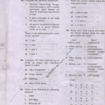
13. AI can be defined as abranch of computer science
a. Concerened with creating computer system exhibiting intelligence
b. Used for creating databases
c. Dealing with graph theory
d. Dealing with artificial data structurers
Ans- a
14. A prescribed set of well defined rules or processes for the solution of a problem in a series of steps is
a. Flow chart
b. Program
c. Algorithm
d. System analysis
Ans-algorithm
15. One of the main features that distinguish microprocessors from microcomputers is
a. Words are usually large in microprocessor
b. Word are shorter in microprocessor
c. Microprocessor does not contain I/O devices
d. Microcessor is not fully integrated
Ans-c
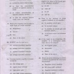
16. What is the principal advantage of using address multiplexing with DRAM memory?
a. Reduced memory access time
b. Reduced requierement for constant refreshing of the memory contents
c. Reduced pin count and decrease in package size
d. No requirement for chip-select input line, thereby reducing pin count
Ans-d
17. The computer language LOGO is based on another powerful list processing language for robotics and artificial intelligence. That language is
a. GSP
b. LISP
c. PASCAL
d. PROLOG
ANS-b
18. The term zero defect is associated with
a. Maintenance
b. Quality control
c. Production
d. Raw materials
Ans-b
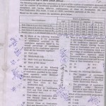
19. The main objective of maintenance is to achieve
a. Increased efficiency of the system
b. Maximum profit from the system
c. Reliability of the system
d. Reduced cost
Ans-a
20. Communication is a process of receiving messages whereas, the process through which we fix meanings to the received message is known as
a. Perception
b. Anchorage
c. Semantics
d. Proxemics
Ans-c
21. Modulation is the process
a. Generating constant frequency radio waves
b. Combining audio and radio frequency waves at the transmitting end of a communication system
c. Reducing distortion in RF amplitude
d. Improving thermal stability of a transistor
Ans-b
22. The bus which is used to transfer data from main memory to peripheral device is the
a. Data bus
b. Input bus
c. DMA bus
d. Output bus
Ans-c
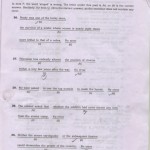
23. Which one of the following statements referring to an interpreter is correct?
a. It has rapid turn around
b. It is faster than complier
c. It occupies less memory space
d. It is preferred for complex calculation
Ans-d
24. Which one of the following is non-verbal communication skill?
a. Writing
b. Eye contact
c. Speaking
d. Reading
Ans-b
25. Which of the following is the defective stage in a TV receiver if their exists a keystone effect in the raster?
a. AGC circuit
b. Horizontal and vertical output circuit
c. Tuner and IF circuit
d. Picture tube circuit
Ans-b
26. A hot smoky product or device is often a sign of
a. Short circuit
b. Ground
c. Open circuit
d. Both ground and open circuit
Ans-a
[TOTAL QUESTION -100, TECHNICAL-67 INCLUDING ELECTRONICS, COMPUTER, MAINTENANCE AND NONTECH-33 INCLUDING PASSAGE , GENERAL APTITUDE TEST]
NOTE- I HAVE DONE ALL THE ANSWER BEST OF MY KNOWLEDGE IF ANY ERROR PLEASE IGNOR IT AND MAIL ME, THANKING U]
REST QUESTION IS UPLOADED SOON————————-
thanks for posting questions asked in dcio exam. Please, post some more questions related to dcio exam.
Hi… Plz post the full papers of 2011, 2012 in pdf or jpeg format
max are wrong. Have u8 ever seen DMA bus, DMA is supported by simple DATA bus so if it is there in option then why to choose DMA bus. It will be right if data bus is not there. and out of compiler interpreter will be fast provided program has no errors since it compiles and executes it.
Thanks.
Could you provide more question papers for the post of
“Deputy Central Intelligence officer Technical Recruitment (DCIO) Test”
Best Regards
Abhishek
For lodging your complaint regarding delay in the selection procedure, you may write a complaint at http://helpline.rb.nic.in/GrievanceNew.aspx .
These delay are put in order to dilute the attention of interested public, so that they can sell the posts or award them to their near-and-dear ones.
The result is supposed to be displayed at http://www.upsc.gov.in .
Please have a look at this poorly maintained site.
I could not see the DCIO 2010 results on UPSC, did i miss them or the results displayed anywhere else…
what may be the cutoff… i am scoring 54+…
Thank you
They have not displayed the results yet..if you find it any where just updates your friends here…